Scitek offers a wide range of instrumentation for surface and material analysis. Our solutions range from experimental highly scientific analysis to high throughput solutions for central facilities. This part of our product range compliments our range of fabrication solutions, so our customers are able to analyse the materials they made.
Electron Spectroscopy

Electron Spectroscopy refers to a group of techniques used to analyse the energy distributions of electrons emitted from or scattered by a sample. In 1983, two years after receiving the Nobel Prize – Professor Kai Siegbahn co-founded Scienta for the continued development of electron spectrometers and systems. PES, or Photoelectron spectroscopy is a tool that has been developed for measuring the chemical and electronic states in different materials. The technology has developed into different directions, including ARPES for electronic structure, HAXPES for analysis of chemical states in the bulk of materials and APPES for analysis of gas-solid and liquid-solid interfaces.
Angle-Resolved Photoelectron Spectroscopy (ARPES)
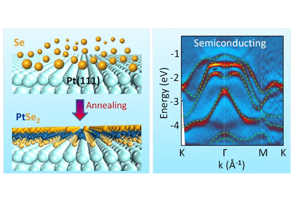
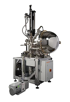
Angle-Resolved Photoelectronspectroscopy (ARPES) has emerged as the most powerful technique to understand the electronic structure of materials and what can influence their physics and chemistry.
Angle-Resolved Photoelectronspectroscopy (ARPES) has emerged as the most powerful technique to understand the electronic structure of materials and what can influence their physics and chemistry.
The electron analyser is a central component in any photoelectronspectroscopy setup. Scienta Omicron offers analysers with outstanding sensitivity and resolution as part of tailored systems and as individual components. Research groups choose our components to build their custom setups located in advanced research laboratories, or at synchrotron beamlines all across the world. With these analysers, spatially resolved chemical state mapping with XPS is possible even at ambient pressures (APPES) and up to atmospheric pressure. Analysers for ARPES applications enable spin resolved electronic band structure mapping across the surface Brillouin zone- thus extending the measurement capabilities for phenomena such as superconductivity, topological insulators, and other interesting quantum materials for spintronic devices.
X-Ray Photoelectron Spectroscopy (XPS)
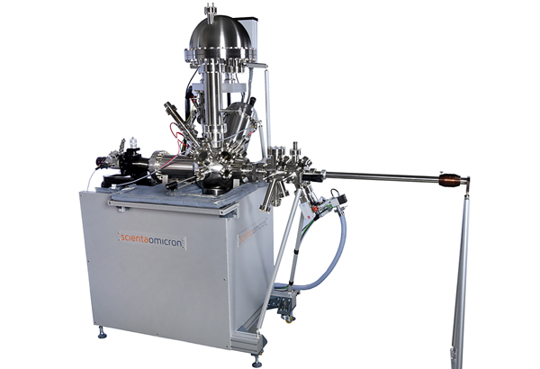
X-Ray Photoelectron Spectroscopy (XPS), also known as ESCA (Electron Spectroscopy for Chemical Analysis) is a surface sensitive quantitative spectroscopic technique. Itis used to measure the elemental composition, chemical state, and electronic state of the elements within a material. XPS is extremely surface-sensitive, typically probing the top 1- 10 nanometers of the material. Applications of XPS span the disciplines of Chemistry, Material Science, Electronics, Catalysis, and Thin Films. PHI offer a fully integrated multi-technique platform with an array of optional excitation sources, sputter ion sources, and sample treatment and transfer capabilities- with a patented monochromatic, micro-focused scanning X-ray source. This offers high sensitivity and high throughput for large area and small area down to 5 um and unique high-throughput non-destructive depth profiling using optional hard X-ray Cr source. A suite of specialised solutions for in-situ characterisation of advanced materials is available, including for example UPS, LEIPS,REELS from the same sample spatial location to measure electronic band structure of organic and inorganic materials. Lab based XPS systems from Scienta Omicron will offer exceptional value and outstanding quantitative XPS performance and ease of operation. Typical systems can host complimentary surface analytical techniques like AES and UPS to enhance its characterisation capabilities. Systems are designed to also cater for analysis under elevated pressures of several mbar, including a specialised system capable of XPS at > 1 bar of pressure to study catalytic reactions.
HAXPES
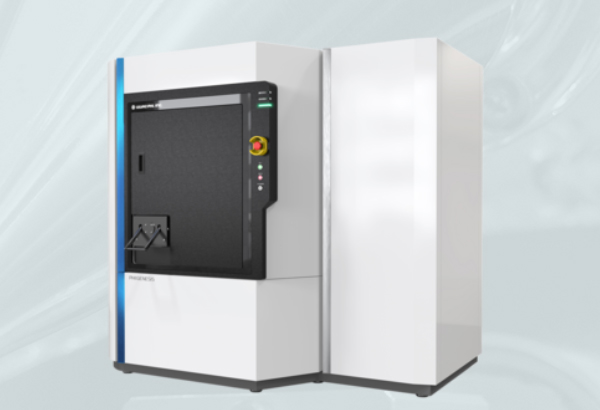
The fully integrated multi-technique platform from PHI offers an arrange of optional excitation sources, sputter ion sources, and sample treatment and transfer capabilities. Hard X-ray Cr Kalpha source provides for depth analysis roughly 3 times those obtained using an (soft) Al X-Ray source. Obtaining spectra from both hard and soft X-Ray sources simultaneously, and from the same sample allows chemical information from surface and near surface depths and without ion beam sputtering. One historically popular field of research is 2D materials. Graphene is one example, being a two-dimensional material consisting of a single layer of carbon atoms arranged in a hexagonal lattice. MXenes, Transition Metal Dichalcogenides, Phosphorene (Black Phosphorous) and Hexagonal Boron Nitride are also other fascinating materials commonly analysed. One growing field of analysis in HAXPES is novel energy-related materials (such as batteries, fuel cells and solar cells) – XPS has become one of the main characterisation techniques scientists will use in their discovery of novel battery materials.
Auger Electron Spectroscopy
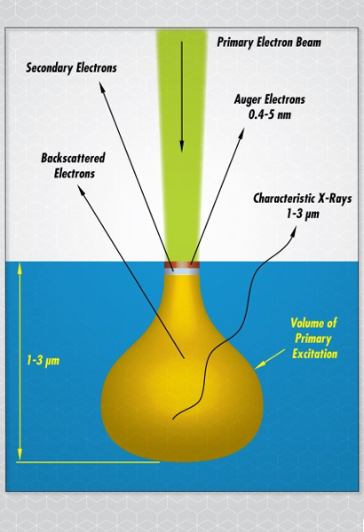
Auger Electron Spectroscopy is a surface-sensitive imaging and analytical technique used to study the elemental composition and chemical state of the surface of materials. When a sample is excited using X-Rays in the range of 2-10keV, ionised atoms undergo a release of Auger electrons with a characteristic kinetic energy. With magnification of 500,000x and higher, our systems provide superior imaging performance as well as spatial resolution, sensitivity, and spectral energy resolution needed to address the worlds most demanding AES applications.
Systems can be enhanced via:
FIB (Liquid metal Focused Ion Beam) allowing in-situ cross-sectioning EDS (Energy Dispersive X-ray Spectroscopy) detection giving qualitative and quantitative elemental information BSE (Backscattered Electron Detector) provides topographic details of the sample EBSD (Electron Backscatter Diffraction) detection provides information about crystal structure and grain orientation.
Photoemmission Electron Microscopy (PEEM)
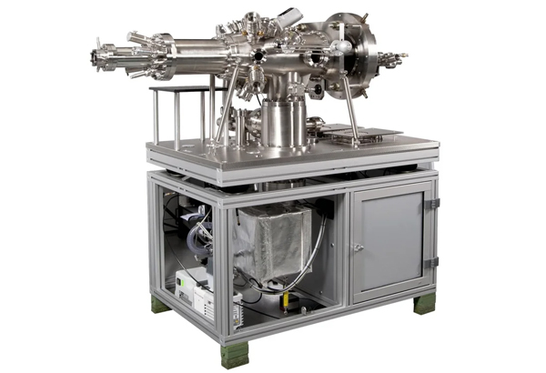
Photoemmission Electron Microscopy, is a powerful imaging technique that combines the principles of electron microscopy and photoemission spectroscopy to combine study of the morphology, chemical composition and electronic structure of materials at high spatial resolution. The NanoESCA from Scienta is an energy-filtering photoemission microscope that can easily switch between the imaging of momentum space and the real space of photoemission electrons. Photoemission has a history as one of the leading techniques in material and surface science. Momentum Microscopy describes the combination of a photoemission electron microscope(PEEM) with an imaging band-pass energy filter. For kinetic electron energies up to 40 eV themicroscope collects all photoelectrons emitted into the complete solid angle above the sample surface. For a discrete energy (selected by the band-pass filter) it forms an image of the photoelectron distribution as a function of the lateral momentum (kx, ky). For example, it is possible to see a full Brillouin zone for certain energies, (e.g. the Fermi surface) in one shot. In live-view mode, it is possible to navigate through the band structure, zoom into details or adjust apertures. By scanning a range of energy filtered momentum maps, one directly gets a 3D data cube (lateral electron momentum vs. electron binding energy) which represents the accessible electronic band structure of the material under investigation. In the last decade, 2D k-space imaging or “Momentum Microscopy” has become one of the late stand most promising developments in this field. It allows a more unique insight into the electron band-structure of novel material systems. Noting that band structure is the key to understanding the working principals of nearly all solid-state devices (transistors, microprocessors, LEDs, solarcells, etc). Scienta’s Momentum Microscopy systems provide fast band structure mapping, which is becoming essential for device engineering in the future.
Time-of-Flight Secondary Ion Mass Spectrometry (TOF-SIMS)
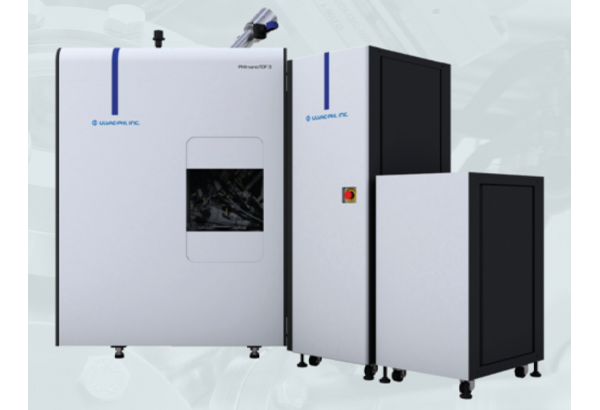
TOF-SIMS is accomplished by exciting a samples surface with a finely focused ion beam which causes secondary ions and ion clusters to be emitted from the samples surface. A time-of-flight analyser is used to measure the exact mass of the emitted ions and clusters. From the exact mass and intensity of the SIMS peak, the identity of an element or molecular fragments can be determined. The average depth of analysis for a TOF-SIMS measurement is approximately 1 nm. Physical Electronics TOF-SIMS instruments provide an ultimate spatial resolution of less than 0.1 μm. Spatial distribution information is obtained by scanning a micro focused ion beam across the sample surface. Depth distribution information is obtained by combining TOF-SIMS measurements with ion milling (sputtering) to characterize a thin film structure. In addition, the Physical Electronics TOF-SIMS instrument provides a unique 3D analysis capability (with use of optional Ar, O2, Cs, C60, Ar cluster, and Ga-FIB ion beams), that combines in-situ focused ion beam sectioning with high mass resolution and high spatial resolution imaging (HR) to provide 3D chemical characterization. The information TOF-SIMS provides about surface layers or thin film structures is important for many industrial and research applications where surface or thin film composition plays a critical role in performance including: nanomaterials, photovoltaics, polymer surface modification, catalysis, corrosion, adhesion, semiconductor devices and packaging, magnetic media, display technology, thin film coatings, and medical materials used for numerous applications.
Physical Electronics TOF-SIMS instruments function in a manner analogous to SEM/EDS instruments that use a finely focused electron beam to create SEM images for sample viewing and point spectra or images for compositional analysis, and with a typical analysis depth of less than 2nm and is therefore better suited for the compositional analysis of ultra-thin layers and nanoscale sample features. The PHI nanoTOF 3 can be configured with a wide variety of options to optimize performance for organic materials, inorganic materials, or both, depending on customer requirements.
Micro-XRF
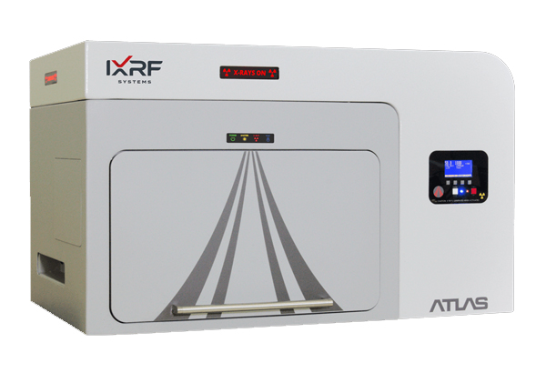
X-Ray fluorescence (XRF) Spectroscopy is a non-destructive technique used to determine the elemental composition of materials. Elements from Beryllium to Uranium can typically be detected, and the energy measurement and peak intensity allows for both quantitative and qualitative analysis of the elements in the sample. Our micro-XRF spectrometer technology introduces a new world of x-ray mapping and automation – boasting the largest chamber volume and SDD detection area (150 mm 2) as well as the smallest spot size of 5 um available with anti-halo optic. Measurements can be performed in Air, or controlled Helium and Vacuum Environments. Additionally, almost anything can be analysed from solids, liquids to powders and particles.
Scanning Probe Microscopy
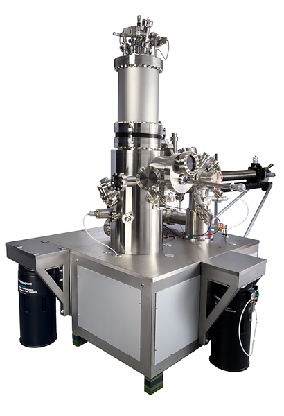
In 1987 – only one year after the Nobel Prize was awarded to Gerd Binnig and Heinrich Rohrer- Scienta Omicron created the legendary STM 1. Scanning Tunneling Microscope (STM) operates upon the principle of quantum tunnelling, measuring the tunnelling current between a conductive tip and a conductive or semiconductive sample. It requires maintaining a constant distance between the tip and the surface that provides atomic-scale resolution of the surface.
Our modern SPM’s offer the ultimate in mechanical stability, ultra-long hold times at liquid helium temperatures, options for strong magnetic fields in a flexible and customisable UHV system environment. Scienta have crafted optimised instruments to ensure outstanding signal qualities for STM operation to ensure excellent results in all relevant scanning and spectroscopy modes. Most advanced techniques for new experiments, such as tip enhanced Raman, scanning tunnelling luminescence, time resolved STM and electron spin resonance experiments, are enabled through adequate optical solutions or high frequency wiring. We can also offer the most advanced dry-technology facilitating convenient low temperature SPM operation without the need for cryogen liquids. To complement the systems Scienta have developed new and advanced controller technology enabling a QPlus operation mode called QPEED simplifying operation and thus ensuring excellent results. The QPlus sensor is a specially engineering tuning fork that has been optimised for high resolution, manufactured with start-of-the-art wafer and lithography techniques- allowing for NC-AFM with simultaneous STM high-resolution measurements.
Atomic Force Microscopy (AFM)
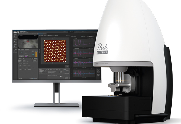
Atomic Force Microscopy (AFM) is a high-resolution imaging technique used to measure and manipulate materials at the nanoscale. It is arguably the most versatile and power microscopy technology for studying samples at nanoscale. Why is it versatile, because an atomic force microscope can not only image in three-dimensional topography, but it can also provide various types of surface measurements to the needs of scientists and engineering. It is powerful because the atomic force microscope can generate images at atomic resolution with angstrom scale resolution height information – and with minimal sample preparation. It is widely used in materials science, biology, and nanotechnology due to its ability to provide three-dimensional surface profiles with atomic or near-atomic resolution. Our latest applications include: Semiconductor research, polymer studies, metal and ceramic processes, thin film advancements, life science interactions, 2-D materials, and facilitating surface engineering. The solutions we provide from Park Systems range from Research AFM instruments for various nano scientific research applications up to Industrial AFMs that are fully automated in-line systems for semiconductor and industrial applications. In addition, Active Vibration Isolation systems are available for enhanced measurement data quality. Park AFM’s feature a comprehensive range of scanning modes so you can collect a wide arrange of data types accurately and efficiently. From the worlds only true non-contact mode that preserves tip sharpness and sample integrity to advanced Magnetic force Microscopy, Park offer the most innovative and accurate models in the AFM industry.
Imaging Spectroscopic Ellipsometry
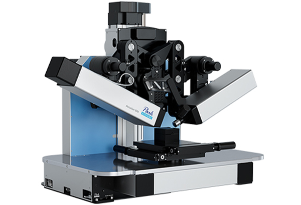
Ellipsometry is an optical technique used to measure the thickness and optical properties (e.g. refractive index and extinction coefficient) of thin films. Park’s Imaging Spectroscopic Ellipsometers combine the benefits of ellipsometry and optical microscopy in a single device. The unification of the two technologies creates a unique metrology tool that redefines the limits of both ellipsometric measurements and polarization-contrast microscopy. The enhanced spatial resolution of imaging ellipsometers (about 1 μm) expands ellipsometry into new areas of microanalysis, microelectronics, and bio analytics. Imaging Ellipsometry is an all-optical, non-contact metrology technique that excels at the layer-thickness and material characterization of micro-structured thin-film samples and substrates. The technique combines microscope imaging with the measurement principles of spectroscopic ellipsometry. It reaches a spatial resolution of about 1 μm, easily beating the limits of other optical metrology tools such as regular ellipsometers or reflectometers. The measurement is based on the sample’s interaction with polarized light. By means of computational modelling, the measured polarization properties translate into maps of the physical sample properties like layer thickness, refractive index and absorption, roughness or anisotropy.
Spectroscopic Ellipsometry
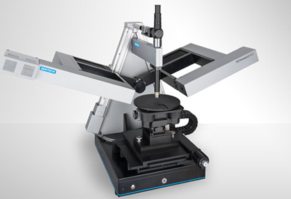
Spectroscopic ellipsometry is an advanced form of ellipsometry that involves measuring the change in polarization of light as it reflects off a sample over a range of wavelengths. This precise and non-destructive technique provides more detailed and comprehensive information about the optical properties and thickness of thin films compared to single-wavelength ellipsometry. Sentech’s Spectroscopic Ellipsometers use fast FTIR ellipsometry up to a wavelength of 3500 nm. It therefore provides the broadest spectral range with the best signal-to-noise ratio and the highest selectable spectral resolution. Silicon films up to 200micron thickness can be measured.
Referenced Spectroscopic Ellipsometry
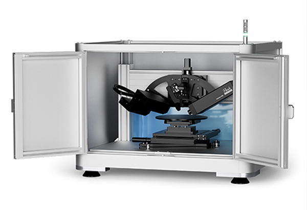
Referenced Spectroscopic Ellipsometers (RSE) are offered by Park Systems offering rapid thickness mapping for quality control. The references spectroscopic ellipsometer combines high sensitivity with the measurement speed of a reflectometer, and exceeds it. In comparison to a laser ellipsometer, it includes the spectroscopic information between 450 and 900 nm. This is important in the event that more than one parameter of the processed layer is variable, for instance thickness and optical density. The reference method is superior to conventional ellispsometry when very thin layers are in focus.
Laser Ellipsometry
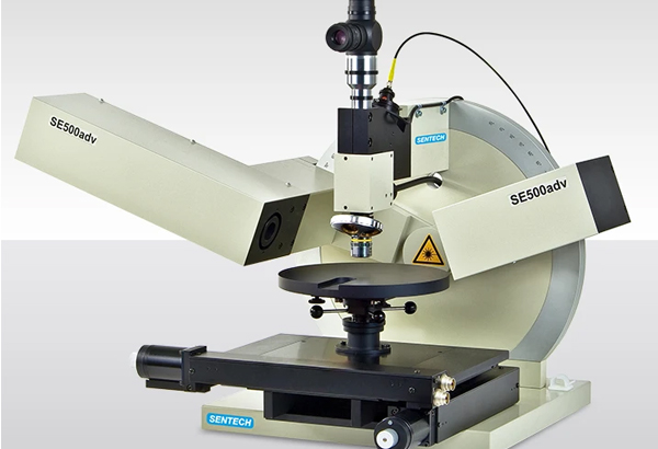
Laser Ellipsometry is a type of ellipsometry that uses a laser as a light source to measure thickness and optical properties of thin films, by leveraging the coherent and monochromatic nature of laser light to achieve high precision and sensitivity. This technique is popular in semiconductor manufacturing and broadly the material sciences where superior accuracy is required. Sentech’s Multiple angle Laser Ellipsometer measures thickness and refractive index of transparent thin films, featuring measurement speed, the stabilised HeNe laser guarantees sub-Angstrom precision in thickness, and with high precision alignment and goniometer accuracy in refractive index determination is easily achieved.
Gas Analysis
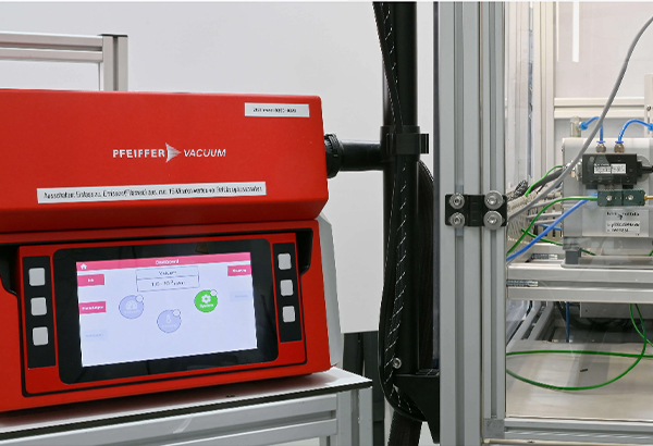
Mass spectrometry identifies and quantifies gas components based on their mass-to-charge ratios. This process involves ionising gas molecules, separating ions based on mass, and measuring their quantity. The technology is widely used in research, environmental monitoring, and industrial applications. Pfeiffer Vacuum’s mass spectrometers provide valuable insights into gas composition, enabling precise quality control and process optimization for various industries. Their range detects and measures trace gases, isotopes, and impurities with exceptional accuracy.


